
Google TPU: From Internal Accelerator to AI Cloud Weapon
How Google’s Tensor Processing Unit evolved from an internal inference ASIC into a serious AI infrastructure platform, where it wins, where it still struggles, and why the real competition with NVIDIA

The market often treats AI accelerators as a simple spec-sheet contest. In that framing, the question is straightforward: which chip has the most compute, the most memory bandwidth, or the highest benchmark score? But that framing is too narrow. The modern AI stack is no longer built around isolated devices. It is built around tightly integrated systems that combine silicon, memory, interconnect, compilers, inference software, data center power, and cooling. Once the unit of analysis shifts from the chip to the system, Google’s TPU story looks far more important than it did in the early years of the market.
Core thesis: TPU is not broadly superior to GPU. It is economically superior when workload regularity, deployment scale, and software control are high enough for system-level optimization to matter.
Today, we take a comprehensive look at Google’s TPU platform and its growing role in AI infrastructure. Over the course of this article, you will gain a clear understanding of the following topics:
The history and evolution of Google TPUs
What a TPU is and how it works
Google’s commercial progress and TPU deployment momentum
TPU–GPU differences in architecture and system design
TPU–GPU comparisons in performance and utilization
TPU–GPU comparisons in cost-performance and full-data-center TCO
What TPUs mean for the competitive landscape of AI infrastructure
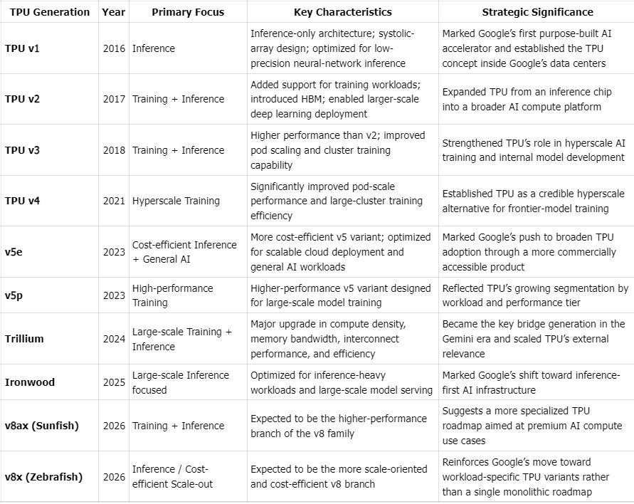
Section 1: A Brief History of the TPU
Google introduced the Tensor Processing Unit (TPU) in 2016 as an internal ASIC optimized for neural-network inference. Its early use cases included Search, Ads, and YouTube recommendation workloads, where dense matrix operations and predictable inference patterns made specialized hardware more efficient than general-purpose CPUs or GPUs.
Over time, TPU evolved well beyond that initial role. The platform moved from inference-only hardware to training-capable accelerators, then to pod-scale systems, and eventually to a broader cloud platform that now serves both internal workloads and external customers. In strategic terms, TPU’s evolution can be read as a sequence of shifts: from internal acceleration, to cloud differentiation, and increasingly to external commercialization.
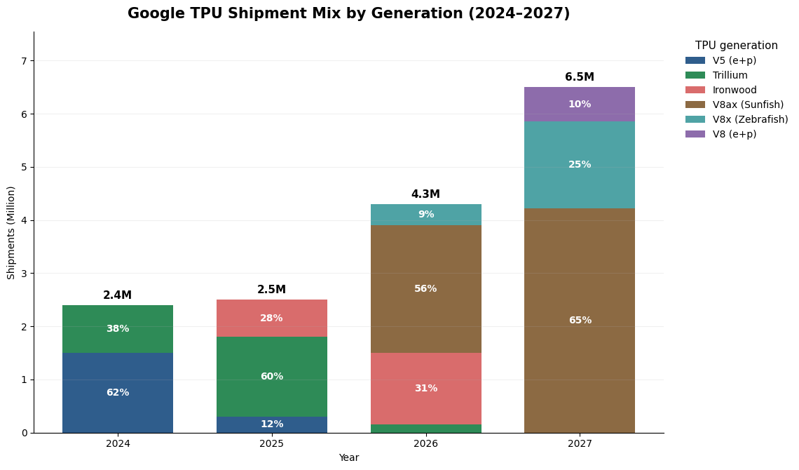
The broad progression is clear. TPU v1 was inference-only and built around low-precision matrix operations. TPU v2 and v3 added training support and high-bandwidth memory. TPU v4 marked the emergence of pod-scale deployment and serious competition with NVIDIA in large training environments. Later generations introduced clearer segmentation across training and inference use cases, alongside higher performance-per-watt and stronger large-model efficiency. Looking ahead, market expectations point to a continued separation between high-end training systems and more cost-optimized inference-oriented SKUs, although the exact future product roadmap should be treated with caution unless explicitly confirmed by Google.
TPU Generations
Section 2: TPU Design and Features
Google’s TPU architecture is fundamentally designed around system-level efficiency rather than single-chip peak performance, reflecting a philosophy that diverges sharply from general-purpose GPU design.
Compute Core: Systolic Arrays and Dataflow Optimization
At the heart of each TPU lies a large-scale systolic array (Matrix Multiply Unit, MXU), purpose-built for dense linear algebra operations. Unlike traditional SIMD/SIMT architectures, TPUs adopt a dataflow-driven execution model (often weight-stationary), minimizing data movement and maximizing reuse within the array. This approach significantly improves efficiency for transformer-based workloads, where matrix multiplications dominate compute cycles.
Interconnect: Scaling as a First-Class Design Goal
TPUs are architected as distributed systems from the ground up. Through a custom Inter-Chip Interconnect (ICI) and integration with optical circuit switching (OCS), TPU pods can scale to thousands of chips with high-bandwidth, low-latency communication. This enables tightly synchronized distributed training and high-throughput inference, effectively treating the pod - not the chip - as the primary unit of computation.
Memory Architecture: Bandwidth as the Bottleneck
Memory architecture is equally central to TPU design. In modern AI workloads, the bottleneck is often not peak compute, but the ability to keep compute units continuously fed with data. TPUs address this not simply through high-bandwidth memory, but through a broader dataflow-oriented architecture that reduces data movement and improves bandwidth utilization. As a result, TPUs can be especially efficient on regular, matrix-heavy workloads such as large language model training and inference.
Hardware–Software Co-Design
These hardware decisions are inseparable from the software stack. TPU performance depends heavily on Google’s broader ecosystem, particularly XLA, JAX, and TensorFlow. Because optimization is compiler-led, Google can analyze larger portions of the computation graph before execution and apply global transformations that are difficult to achieve in a more general-purpose runtime model. This includes fusing multiple operations, minimizing intermediate memory writes, controlling tensor layout, and mapping workloads more directly onto systolic arrays and on-chip memory. In practice, this hardware-software co-design is one of the main reasons TPU systems can achieve high realized utilization at scale, especially on regular, matrix-dominated AI workloads.
Efficiency vs Flexibility Trade-off
The trade-off, however, is clear. TPU architecture delivers strong performance-per-watt and attractive cost efficiency in large, well-optimized deployments, but it is less flexible than GPUs for irregular, dynamic, or rapidly changing workloads. Its advantages are most pronounced when workloads are highly structured, models are large and relatively stable, and execution can be optimized end to end through the compiler.
In summary, TPUs should be understood not as isolated chips, but as tightly integrated systems. Their true advantage emerges not from peak FLOPs on a single device, but from co-optimizing compute, memory, interconnect, and software across thousands of chips, enabling Google to deliver AI at hyperscale with superior efficiency and economics.
Section 3: Commercialization
TPU’s commercial significance has increased because its customer base is no longer limited to Google itself. What was once predominantly internal infrastructure is increasingly becoming a hybrid platform serving internal products, Google Cloud customers, and a growing set of strategic external partners. That shift matters because it turns TPU from a cost-saving internal asset into a platform that can also generate cloud revenue and strengthen Google’s position in the broader AI infrastructure stack.
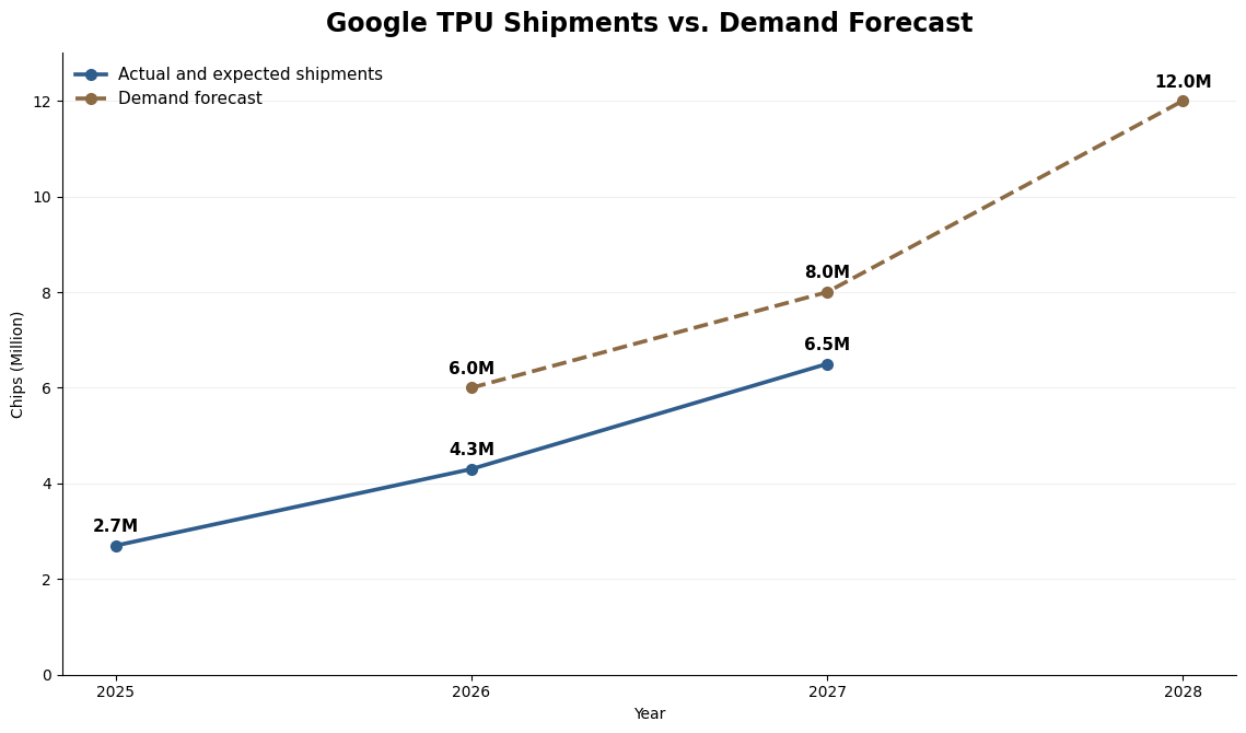
Shipments and Forecasts
TPU shipment volumes have scaled rapidly, with generation transitions occurring at a very fast pace. At this stage, growth appears to be constrained less by end-demand than by supply-side bottlenecks, particularly advanced packaging capacity such as CoWoS.
Customer Mix
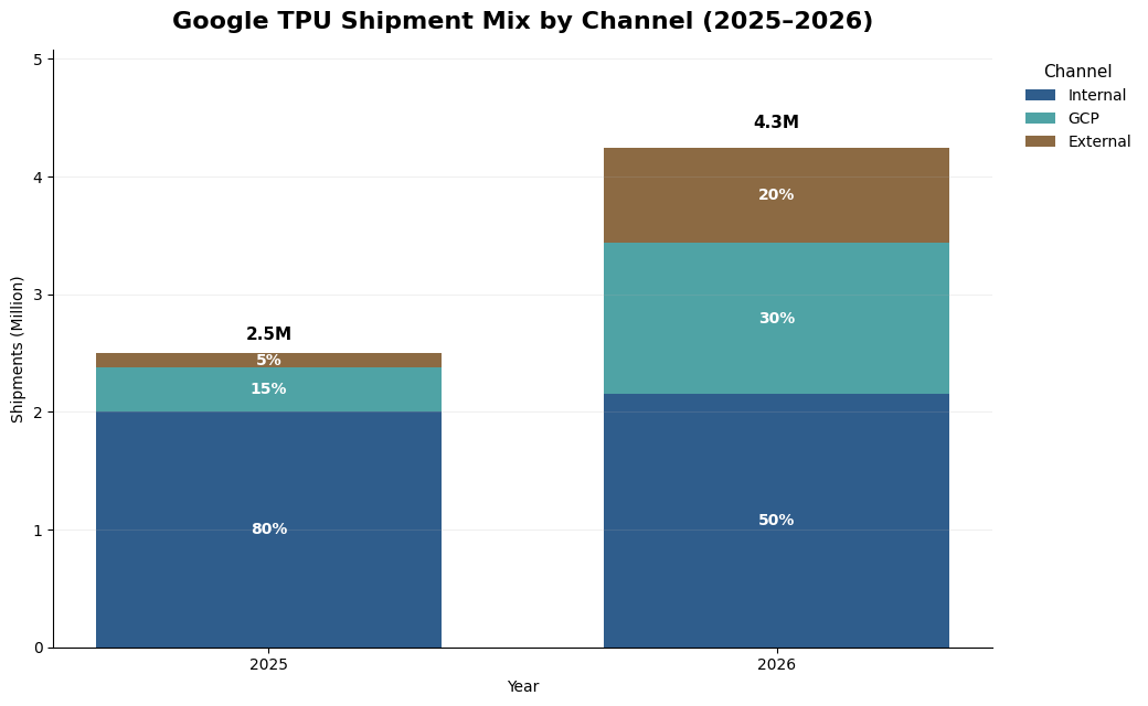
Google’s TPU deployment is increasingly shaped by a hybrid consumption model, spanning internal workloads, cloud customers, and a fast-growing set of strategic external partners. What was once a predominantly internal infrastructure has evolved into a commercialized AI platform with rising external demand.
Internal Google: A large share of TPU capacity is still dedicated to Google’s own products and services, including Search, YouTube, Ads, and Gemini. Industry estimates suggest that in 2025, internal usage accounted for roughly 80% of total TPU shipments, highlighting that TPU was still primarily an internal infrastructure asset. By 2026, internal shipments are expected to remain stable, but the share of total volume declines sharply to around 50% as external-facing demand accelerates. Internal usage therefore remains strategically important, but it is no longer the sole driver of the TPU scale.
Google Cloud Platform: TPUs are becoming a more important differentiator for GCP, particularly in large-scale AI workloads where price-performance matters. Our channel work suggests GCP-related TPU increase from about 15% in 2025 to roughly 30% of total shipments in 2026. This suggests that Google Cloud is moving from a secondary channel to a major source of TPU commercialization. The customer base includes both enterprise workloads and AI-native model developers that access TPUs through Google-hosted infrastructure. Importantly, this category also includes large strategic customers that obtain TPU capacity through a rental model rather than direct ownership, such as Meta and Anthropic. As a result, part of what appears as GCP consumption is in fact strategic external demand delivered through Google’s cloud channel.
External Strategic Customers: We define external sales as the direct purchase of TPUs for deployment in customer-owned data centers. This remains a small channel in 2025, at around 5% of total shipments, but scales rapidly to nearly 20% of total volume in 2026, according to industry estimates. The sharp increase suggests that TPU adoption is beginning to move beyond internal deployment and cloud rental toward more strategic, customer-owned infrastructure. In many cases, large customers appear to follow a progression: first renting or testing TPUs through cloud access, then moving toward direct deployment once performance and economics are validated.
Large External Customer
Anthropic
The partnership between Anthropic and Google Cloud is a structurally complex AI infrastructure agreement, combining direct hardware procurement with long-term cloud capacity commitments. Anthropic plans to deploy up to ~1 million TPUs, with a significant portion sourced as rack-level systems directly from Broadcom, alongside large-scale consumption through Google Cloud. The relationship is structured as a hybrid model: Anthropic secures baseline capacity and control via owned infrastructure, while leveraging GCP for elastic scaling, orchestration, and managed services.
Recent disclosures from Broadcom indicate that direct hardware orders have expanded beyond initial expectations - from ~$10B to ~$21B, implying a substantial increase in Anthropic-owned TPU capacity and signaling a strategic shift toward partial vertical integration of compute. At the same time, Google captures the majority of economic value through cloud services, with an estimated ~$42B+ in committed GCP spend (RPO) tied to TPU usage. This dual structure effectively transforms the partnership into a long-term reservation of AI manufacturing capacity, where Anthropic secures supply in a constrained market, and Google locks in demand to justify continued infrastructure buildout.
Anthropic TPU Adoption Roadmap
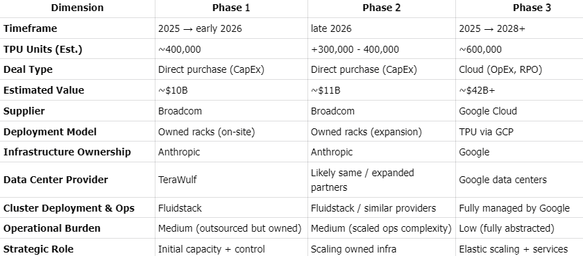
Meta
The commercial rationale behind this cooperation is straightforward. Meta and Anthropic share certain similarities at the model level, and Meta’s Llama roadmap, like Google’s Gemini, is increasingly associated with architectures that benefit from large-scale, highly efficient AI accelerators, including MoE-like design approaches. Google has already demonstrated that Gemini can run effectively on TPUs, with clear economic benefits in both training and inference. Against that backdrop, Meta wants to test whether Google’s TPU platform can deliver better value than NVIDIA GPUs for deploying and scaling Llama. That expected improvement in performance economics is the core business driver behind the partnership. Meta’s cooperation with Google appears to follow a two-phase approach.
Phase 1: TPU rental and technical evaluation in 2026.
Meta is expected to rent Google TPUs in 2026 to test Llama models on the platform. The purpose of this phase is to evaluate how effectively Llama can be adapted to TPUs, including both inference and training workloads. In practical terms, Meta wants to assess whether TPUs can meet the performance, scalability, and efficiency requirements of the Llama family before making a larger infrastructure commitment.Phase 2: Potential TPU procurement for Meta-owned data centers in 2027.
If the testing phase shows that TPUs can support Llama training and inference at the required level, Meta could move to a second stage in 2027 by purchasing TPUs from Google and deploying them in its own data centers. This would mark a shift from short-term evaluation to long-term infrastructure adoption.
Apple
Apple has emerged as a meaningful external buyer of Google’s TPUs, purchasing roughly 100,000 TPU v5p chips in 2024. Demand is expected to accelerate further in 2025, with Apple’s procurement to double to around 200,000 units. This expansion reflects a broader industry shift also seen at Meta, OpenAI, xAI, and Anthropic, as leading AI developers seek to reduce reliance on NVIDIA’s expensive hardware and tightly controlled software ecosystem. Apple’s sustained appetite for Google TPUs has made it one of the most important third-party drivers of Google’s external TPU shipments, underscoring the growing commercial relevance of TPUs beyond Google’s own internal workloads.
OpenAI
OpenAI has begun renting Google TPUs through Google Cloud, but its usage appears to remain at an early testing stage rather than a broad production deployment. At this point, TPUs seem to serve more as a source of commercial leverage in OpenAI’s negotiations with NVIDIA, helping the company push for better GPU pricing, rather than as a core compute platform adopted at scale. More fundamentally, Google’s TPU architecture does not appear to be an ideal fit for OpenAI’s model stack, which likely limits the probability of TPU becoming a major part of OpenAI’s long-term infrastructure strategy.
Others: There is no reliable public evidence so far that Microsoft or xAI are Google TPU customers. In Microsoft’s case, the public narrative remains centered on its in-house Maia accelerator strategy, while xAI continues to be associated primarily with large-scale NVIDIA GPU deployments.
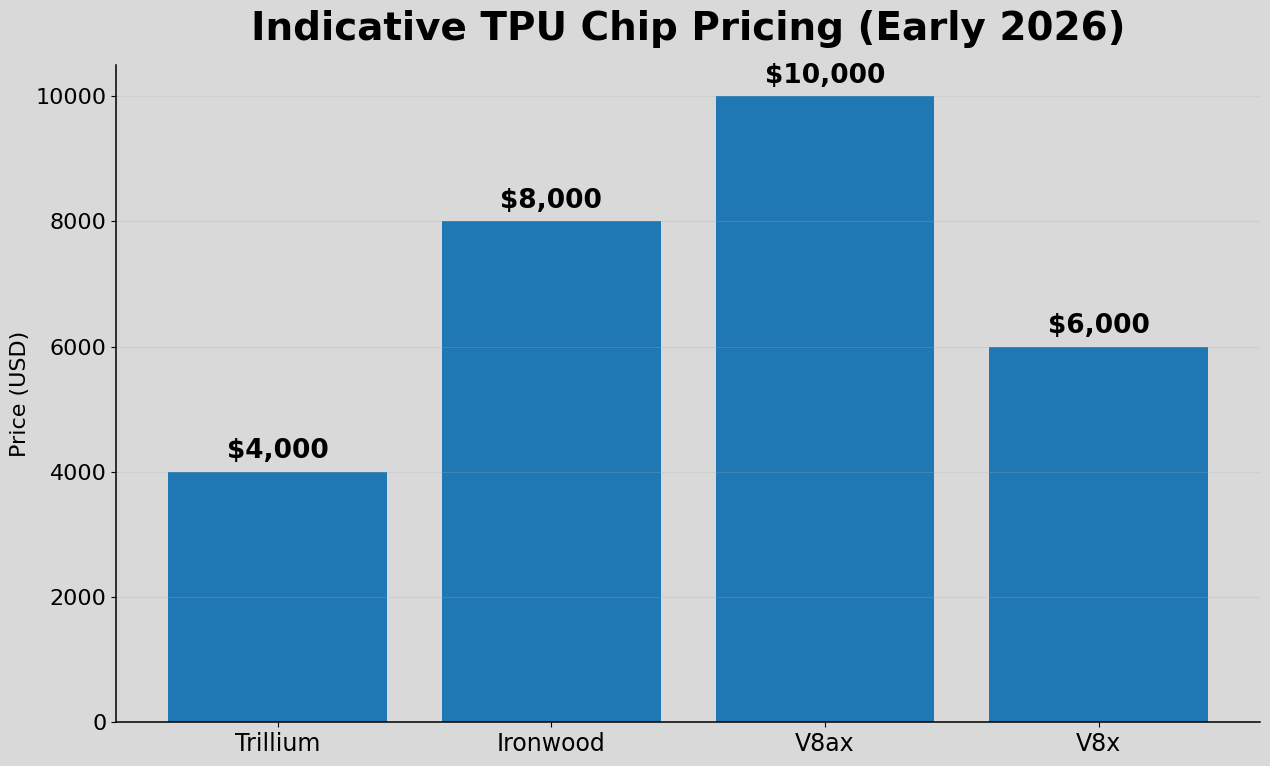
Pricing
Google does not publicly disclose a standard standalone purchase price for TPUs. In practice, TPU economics are more visible through Google Cloud pricing and through directional industry checks than through a public list price. That is an important distinction: cloud pricing, transfer pricing, and end-customer economics are not the same thing, and they should not be treated as interchangeable.
Based on our channel checks, indicative TPU chip pricing in early 2026 - referring to the price charged to Google rather than the price paid by end customers - is as follows. Newer generations are not necessarily more expensive, as pricing appears to be driven more by performance profile and workload positioning than by generation alone.
Profit Margin
Notably, Google appears less focused on maximizing standalone chip margins than Nvidia. Google’s gross margins are estimated at ~20-30% when selling TPU to external customers, with profits shared by suppliers. In contrast, Nvidia has a very stable 75% gross margin thanks to its vertical integration of chip design, software and system
Indicative TPU System Value Capture Structure
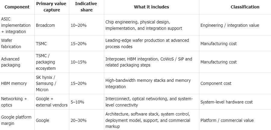
Percentages are illustrative estimates of system cost and are intended for conceptual analysis only. They are not based on company-disclosed cost breakdowns.
Section 3: TPU vs GPU
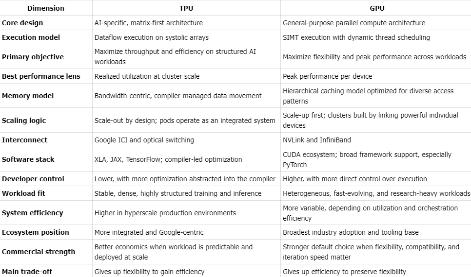
Design
At a high level, both TPUs and GPUs accelerate machine learning workloads. In practice, they are built on very different design assumptions. GPUs prioritize flexibility and broad programmability; TPUs prioritize efficiency and system-level optimization for large-scale AI.
As AI shifts from model development to large-scale deployment, that distinction matters more. The competition is not just between two chips, but between two ways of organizing compute, memory, scaling, and software.
Compute: Flexibility vs. Structured Execution
GPUs are built around a SIMT model, in which many threads execute in parallel under dynamic scheduling. This makes them highly versatile across graphics, scientific computing, and AI. But that flexibility creates overhead: irregular control flow, thread divergence, and scheduling complexity can reduce efficiency on structured workloads such as large matrix multiplications.
TPUs take the opposite approach. They are built around systolic arrays, where data moves through compute units in a predictable pipeline. Execution is organized as dataflow rather than thread scheduling, allowing higher utilization on the dense, repetitive tensor operations that dominate modern AI.
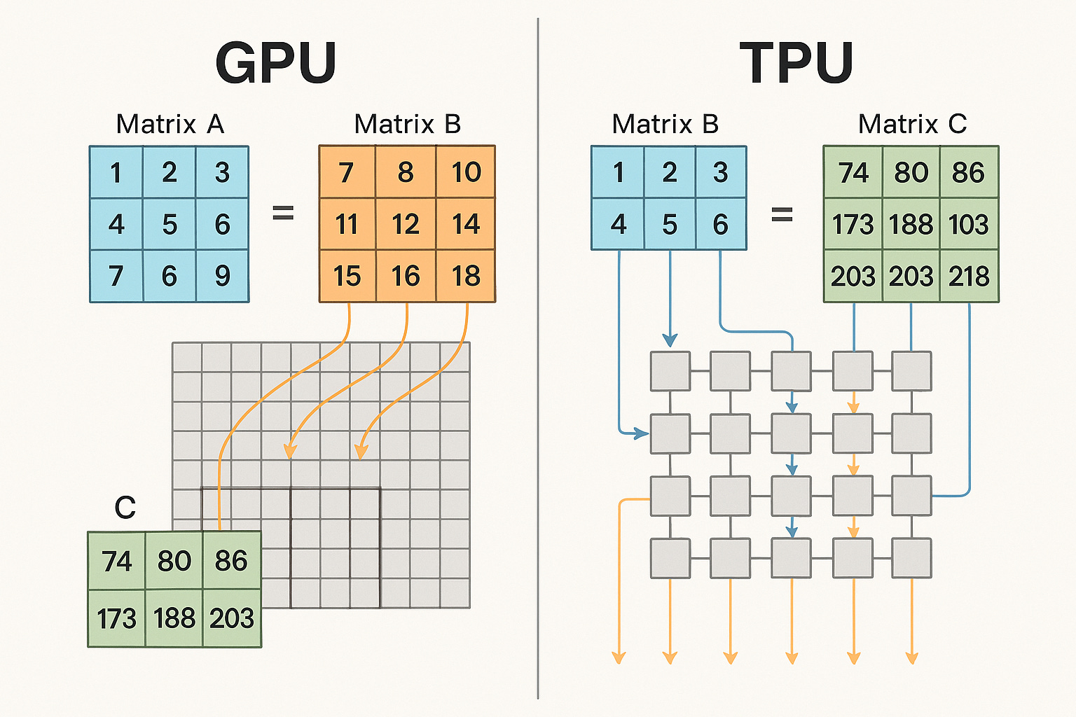
Source: The Savvy Canary
Memory: Bandwidth Matters More Than Raw Compute
In modern AI systems, performance is often constrained less by peak compute than by data movement. GPUs address this with a flexible memory hierarchy that includes HBM, caches, registers, and shared memory. This makes them highly adaptable across many workload types, but it also means efficiency depends heavily on access patterns, kernel design, and how often data must be written back to and read from memory.
TPUs use a more explicit bandwidth-first model. Rather than relying as heavily on dynamic cache behavior, TPU memory movement is planned more directly by the compiler, with HBM tightly coupled to compute and dataflow organized around systolic arrays. The goal is to minimize unnecessary movement, improve locality, and keep matrix units continuously fed with data. Put simply, GPU memory systems are designed to handle many kinds of workloads well, while TPU memory systems are designed to move data in the fewest possible steps for highly structured AI computation.
Scaling: Connected Devices vs. Designed Systems
The contrast becomes clearer at cluster scale, but it is best understood as a difference in fabric design rather than a simple scale-up versus scale-out divide. In NVIDIA systems, NVLink/NVSwitch serves as the high-bandwidth fabric for tightly coupling GPUs within a node or rack, while InfiniBand or Ethernet connects those systems across larger clusters. This gives GPU infrastructure strong modularity and broad deployment flexibility, but cluster performance depends heavily on how well software manages communication overhead and distributed execution.
Google TPU systems follow a similar two-level logic, but with tighter integration at the pod level. ICI acts as the high-bandwidth interconnect within a TPU pod, while larger-scale expansion across pods depends on Google’s broader data center network and optical switching. The practical difference is not that GPUs are “assembled” and TPUs are “designed,” but that TPU pods are more tightly co-designed as an integrated system from the start, with communication and topology optimized around a narrower class of large-scale AI workloads.
Software: Ecosystem Breadth vs. Hardware-Software Co-Design
NVIDIA’s biggest advantage is not just hardware, but software. CUDA, combined with PyTorch and a broad tooling ecosystem, gives developers a mature platform with fine-grained control over kernels, memory behavior, and execution. This has been one of the main reasons GPUs became the default platform for AI development.
TPU software works differently. It relies on a more tightly integrated stack centered on XLA, JAX, and TensorFlow, where developers more often describe computation at a higher level and the compiler takes a larger role in optimization. Instead of depending as heavily on programmer-directed tuning, the TPU stack leans on the compiler to optimize the full computation graph - fusing operations, choosing tensor layouts, reducing data movement, and planning execution ahead of time. In simple terms, GPU performance is often tuned more directly by the programmer, while TPU performance depends more heavily on what the compiler can optimize automatically. That approach can deliver very high efficiency on structured workloads, but within a narrower software ecosystem.
Performance: Peak Throughput vs. Realized Utilization
These design choices lead to different performance profiles. GPUs are often optimized for peak single-device performance and benchmark leadership. In production, however, realized utilization typically falls meaningfully below theoretical limits because of memory bottlenecks, synchronization overhead, communication costs, and workload variability. A commonly cited rule of thumb for large-scale GPU training is utilization around 30%, although well-optimized clusters can achieve materially higher levels in practice.
TPUs, by contrast, are optimized less for peak headline numbers than for sustained throughput across tightly integrated systems. Their advantage is often not higher theoretical performance per chip, but more predictable and efficient utilization at scale, especially on structured, compiler-friendly workloads. Some industry estimates place TPU utilization at roughly 40% in favorable settings, though this should be understood as a scenario-dependent estimate rather than a universal benchmark. In production environments - where cost per query, training efficiency, and energy use matter more than peak FLOPs - that distinction can be critical.
The Core Trade-off
At its core, the TPU-GPU divide is a trade-off between flexibility and efficiency.
GPUs offer a broader ecosystem, greater programmability, and stronger support for diverse or fast-changing workloads. TPUs offer tighter hardware-software integration, better scaling characteristics, and higher efficiency on stable, highly structured AI workloads.
Neither is universally superior. GPUs remain the default where iteration speed, workload diversity, and ecosystem compatibility matter most. TPUs are strongest where workloads are predictable, deployment is hyperscale, and system efficiency matters more than generality.
The TPU vs. GPU debate is often framed as a chip competition. More fundamentally, it is a competition between architectural philosophies.NVIDIA has built the dominant general-purpose AI compute platform. Google has built a more specialized system optimized for delivering AI efficiently at scale.As the industry shifts from training models to serving them economically, the key distinction will increasingly be not peak performance, but realized performance; not flexibility alone, but efficiency at scale.
Comparison between TPU and GPU
Hardware Specs
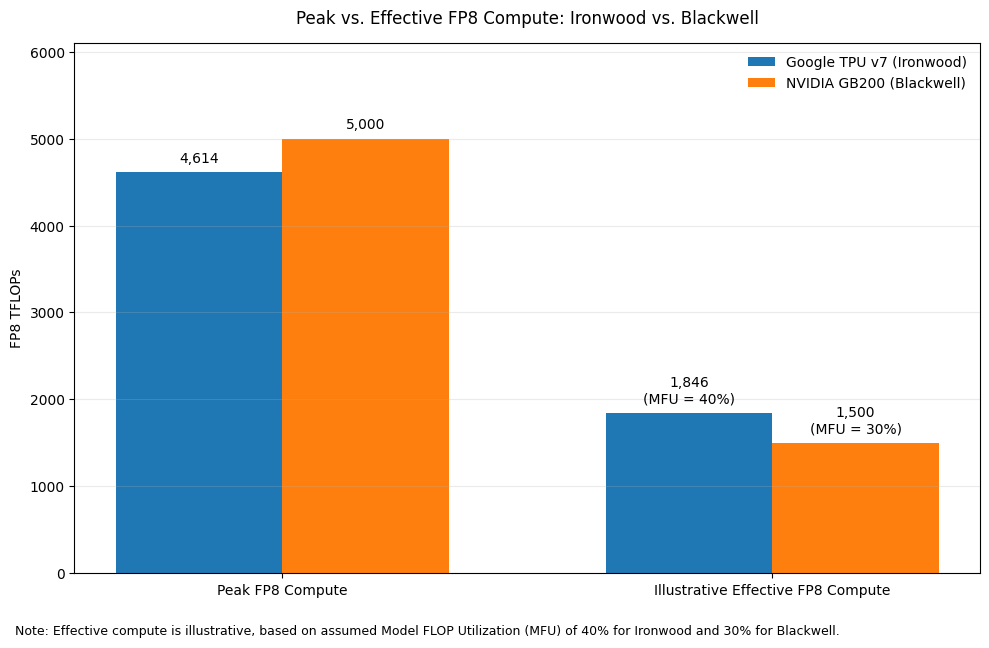
The framework we use is to evaluate the hardware across three dimensions: compute performance, memory subsystem, and interconnect / cluster architecture. Within compute, it is also important to distinguish between peak compute and effective compute. Peak compute refers to the theoretical maximum throughput under ideal conditions, while effective compute reflects the portion of that performance that can actually be converted into useful training or inference work after accounting for memory constraints, communication overhead, software efficiency, and utilization at scale.
Compute performance: The most relevant comparison today is increasingly centered on FP8 throughput, which has become the primary battleground for leading-edge AI accelerators. Google’s latest TPU v7 (Ironwood) has become much more competitive with NVIDIA’s latest Blackwell generation than in prior cycles. According to Google Cloud’s published specifications, TPU v7 delivers 4,614 TFLOPs of FP8 peak compute per chip. By comparison, NVIDIA positions GB200 at roughly 5,000 TFLOPs of FP8 compute, meaning the gap in raw dense low-precision throughput has narrowed materially. For context, the previous-generation TPU v6 (Trillium) offered 918 TFLOPs of dense FP8 compute, which means TPU v7 represents a major generational step-up and a substantial narrowing of the competitive distance versus NVIDIA’s newest platform. In other words, on a pure peak-FLOPs basis, TPU v7 is no longer clearly outclassed by NVIDIA’s flagship platform; instead, the two are now in the same performance tier.
That said, comparing AI chips on FP8 performance requires an important distinction between theoretical peak compute and effective compute. In practice, the headline FLOPs figures marketed by vendors such as NVIDIA and AMD often reflect instantaneous peak performance achievable under favorable conditions, sometimes aided by dynamic voltage and frequency scaling, rather than the level of throughput that can be sustained across real production workloads. As a result, theoretical FP8 performance can overstate what users actually realize in large-scale training. For GPUs, actual utilization of advertised FP8 compute - often measured by Model FLOP Utilization (MFU) - is typically much lower, with real-world training workloads often achieving utilization levels around 30%. By contrast, Google’s TPU architecture is generally viewed as more conservative in how performance is specified, meaning its stated compute is often closer to sustainable delivered throughput. This matters because for highly optimized operators, effective compute can diverge materially from theoretical peak. In particular, elite users such as Anthropic have reportedly been able to push TPU utilization to around 40% MFU through deep system-level optimization, allowing TPUs to deliver very strong effective compute economics even when their headline peak FLOPs remain slightly below NVIDIA’s top-end figures. In other words, while NVIDIA may still lead on nominal peak compute, TPU can be more competitive on usable compute than raw spec-sheet comparisons alone would suggest.
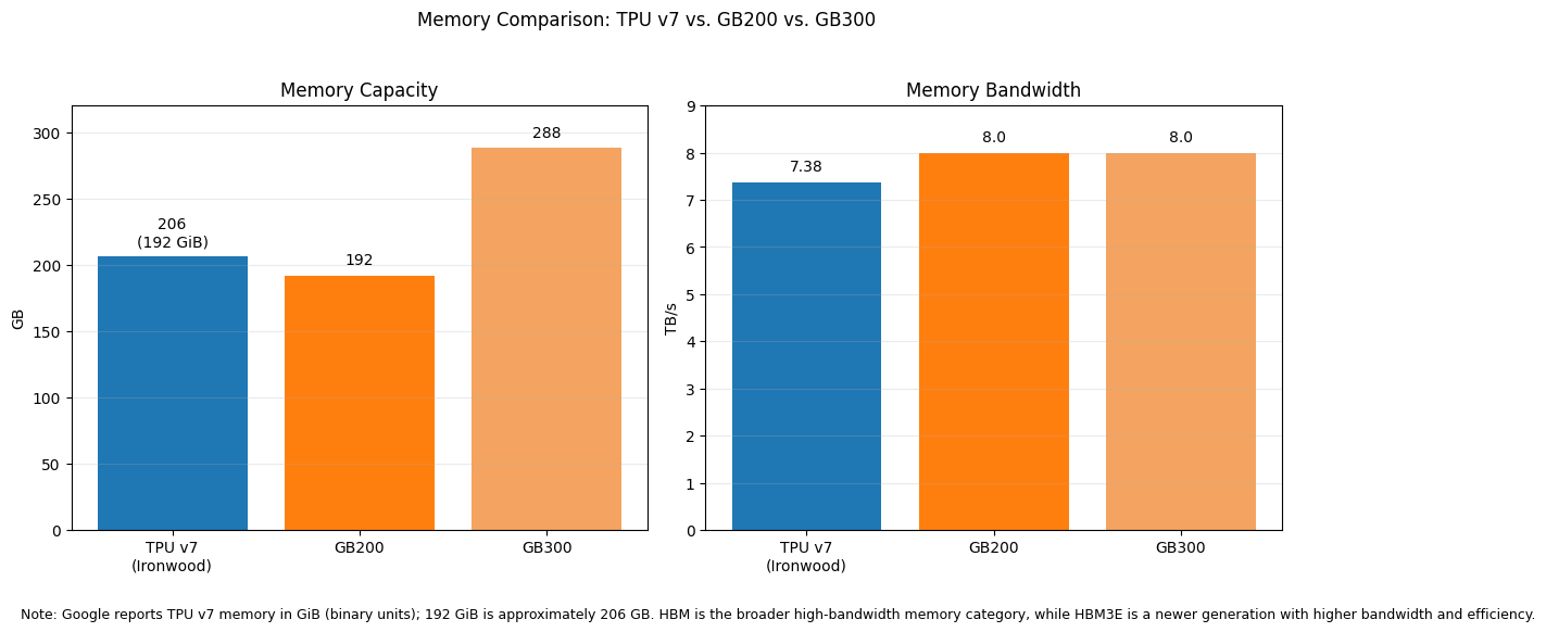
Memory capacity and bandwidth: TPU had historically been at a disadvantage, but that weakness has been substantially reduced in the latest generation. Google states that TPU v7 includes 192 GiB (192 GiB ≈ 206 GB. ) of HBM per chip and 7,380 GB/s of HBM bandwidth, a major step up from prior TPU generations. This means TPU v7 now matches GB200 on memory capacity, as NVIDIA’s Blackwell platform is commonly described with 192GB HBM3E (HBM is the memory category; HBM3E is a newer generation with higher bandwidth and improved efficiency)at the GB200 level. That said, NVIDIA still extends its lead at the upper end with GB300, which raises memory capacity to up to 288GB HBM3E per GPU and bandwidth to roughly 8 TB/s. So on memory, the latest comparison is no longer “TPU far behind GPU”; instead, it is more accurate to say that TPU v7 has reached parity with GB200-class capacity but still trails GB300 at the frontier end of the Blackwell Ultra family.
Interconnect and cluster scale: Google documents that TPU v7 supports pods of up to 9,216 chips, using a topology built around direct inter-chip links and large-scale pod interconnection. By contrast, NVIDIA’s flagship commercial Blackwell system is typically framed around the GB200 NVL72 or GB300 NVL72 rack-scale configuration, which organizes 72 GPUs into a single NVLink domain. NVIDIA’s NVL72 is extremely powerful and highly optimized, but it is still a much smaller native building block than a full TPU pod. This difference matters because at frontier scale, the bottleneck often shifts from single-chip speed to the efficiency of synchronizing thousands of accelerators. In that environment, TPU’s large native cluster design can translate into stronger effective scaling behavior, particularly for workloads that are communication-heavy or require tightly coordinated distributed execution.
Taken together, the latest-generation comparison is much more balanced than older TPU-versus-GPU narratives suggest. NVIDIA Blackwell still appears stronger in software maturity, commercial ecosystem breadth, and top-end memory in its GB300 configuration. But Google TPU v7 has largely closed the gap in peak compute, substantially narrowed the memory disadvantage, and retains an architectural advantage in pod-scale interconnect and large-cluster efficiency. As a result, the most important conclusion is not simply that NVIDIA leads on peak specs or that TPU is cheaper; rather, it is that TPU is now credible on both peak compute and effective compute, especially in hyperscale environments where delivered utilization and system-level scaling matter more than isolated chip benchmarks.
In the paid section of the article, we will continue to discuss:
The software and ecosystem difference between TPU and GPU
What Google has done to catch up in software capabilities and ecosystem
TCO difference of TPU vs. GPU at peak utilization as well as effective utilization
Conclusion and main takeaways
