
CPO Testing Fundamentals
The Hidden Bottleneck Behind Co-Packaged Optics

Testing is currently one of the biggest bottlenecks in CPO production. This article provides a deep dive into the CPO testing supply chain. After reading it, you will understand:
What are tested in CPO testing
Three types of probes in CPO testing, their prices and main vendors
Testing instruments, their prices and main vendors
Key components/ modules of a testing station
How CPO testing differs from EML optical module testing
CPO coupling methods and their implication on testing
Why testing is a major bottleneck for CPO production
Two main competing products/ solutions in CPO testing
Covered companies include: ficonTEC/ RoboTechnik (300757.CH), FormFactor ($FORM), Advantest (6857.JP), Teradyne ($TER), Keysight ($KEYS), R&S ($RSGN), Semight (688808.CH), Focuslight (688167.CH).
Disclaimer: This publication is for informational and analytical purposes only. The views expressed here reflect my personal research and opinions at the time of writing and should not be construed as investment advice, a recommendation to buy or sell any security, or a solicitation to engage in any investment activity. I may hold positions in some of the companies or securities discussed, and my views may change without notice. Readers should conduct their own research and consult a qualified financial adviser before making any investment decisions. Investing involves risk, including the potential loss of principal.
Part 1: PIC Testing
In CPO testing, both electrical and optical signals need to be tested. Around 80% of the test parameters are electrical, but 80% of the complexity lies in optical testing. Therefore, PIC testing is a core part of the overall process.
Part 1.1 Three types of signals
In general, PIC testing covers three types of signals:
Electrical signal testing: A PIC contains components like modulators and photodetectors (PD) that are driven by electrical currents. Thus, electrical signals need to be tested for these components - for example modulators are tested for things like L-I-V curve, threshold current, and voltage to ensure the electrical-to-optical conversion works properly; and PDs are tested for dark current and photocurrent after being applied bias voltage.
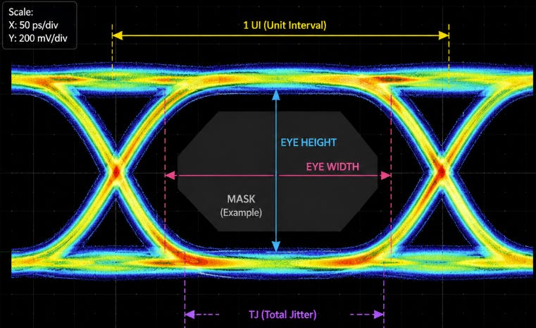
High frequency testing: High-frequency RF signals after modulation are tested to ensure the module can handle high-bandwidth workloads as the light is encoded with data. The testing results include things like eye diagrams, bit error rate, and signal jitter. It is the more complex testing category but also the high-value one. Essentially, it tests how “good” the output signals look before they are sent into fiber networks.
Optical signal testing: Optical signals pass through passive components in the PIC, such as waveguides, switches, and attenuators. During the process, the signals will experience losses (return loss and insertion loss, for example). Therefore, parameters such as optical power and wavelength must be tested to ensure the signals maintain a certain quality level after the whole transmission process.
Part 1.2 Probes
In order to complete the testing, probes are used to send signals to and receive signals from the PICs. Corresponding to the three types of signals, there are three types of probes:
Electrical probes: are quite standard components, as they are also widely used in semiconductor testing - as a result, the technology is very mature. In PIC testing, they are used to provide power to optical components such as modulators, PDs, and lasers, as well as to retrieve electrical signals from the PICs for analysis.
Electronic probes are not expensive - usually, a few thousand dollars is enough for the entire testing station. At that cost, one electrical probe can typically support 500K to 1 million test cycles. However, in CPO testing, its lifespan can be reduced to ~250K cycles as it needs to transmit higher-current signals and faces stricter requirements for cleanliness and wear.
As for suppliers, FormFactor ($FORM) is the premium, industry-benchmark producer, while Chinese companies such as Semight (688808.CH) are gaining market share. The latter’s product quality is good enough for most testing scenarios while offering more competitive prices.
RF probes: are technically a type of electrical probes, but they are used specifically for high-frequency RF signals in testing - they inject or capture high-frequency RF signals from the PIC. These are high-priced products, typically selling for $100K+ per probe. Companies such as FormFactor ($FORM) and R&S ($RSGN) are the main providers.
Optical probes are used for optical signal testing. In terms of physical forms, the probes are typically two fibers coupled very close to the PIC - one for input and one for output. The fibers tips are embedded with microlenses, which are made mainly using two approaches: 3D-printed polymers and polished microlenses. The former is cheaper but more fragile, while the latter is more robust but more expensive. A key company for making the polished microlens is Focuslight (688167.CH).
These microstructures are designed to converge light into fibers for later transmission. They need to be positioned at an extremely precise and close distance from the PICs to minimize optical losses. This process takes a long time and requires high-end, premium, machines, which we will cover in later sections.
One 3D-printed optical probe is sold for around $3,000, while microlens-based probes are sold at higher prices. Major probe providers include FormFactor ($FORM), Technoprobe ($TPRO), Tokyo Electron (8035.JP), and MPI (6223.TW). FORM and TPRO appear to be more advanced than others in CPO optical probe development race.
Part 1.3 Testing instruments
Testing instruments are used to analyze signals captured by electrical and optical probes. For optical modules, the most commonly used instruments are oscilloscopes and Bit Error Rate Testers (BERTs). Oscilloscopes receive and test module’s output signals, typically displayed as eye diagrams, while BERTs are used to send signals and test the performance of the modules’ receiving subassembly capabilities.
Instrument requirement is closely tied to the lane bandwidth it can support. For example, an instrument capable of testing 200G-per-lane signals can sell for more than twice the price of one that supports only up to 100G per lane.
Between the two most common instruments, oscilloscopes are more complex and command much higher prices - For example, BERTs used on production lines may cost around $20K, while oscilloscopes can cost around $200K.
For oscilloscopes, Keysight ($KEYS) is the main vendor in the market, with dominant share in both R&D and production spaces. For BERTs, Keysight remains dominant in the R&D space, where requirements for instrument capability are higher but volume demand is lower, while Chinese firm Semight can now offer good-enough alternatives and is gaining share in the production-line space.
Companies like Keysight also sell testing solutions. For example, Keysight sells its end-to-end silicon photonics testing solutions exclusively to FormFactor, which leverages its probe expertise to build the final integrated solution.
Part 1.4 Testing station
Combine the testing probes and instruments, and you have the testing station. A testing station consists of three parts: the probe module, coupling module, and testing module. The probe module provides electrical and optical probes that send signals to and retrieve signals from the PICs. The coupling module aligns the optical probes with the PICs at micron-level precision; and the testing module consists of instruments that measure and analyze the signals retrieved from the PICs. Different instruments are required for different types of electrical, RF, and optical signals.
The coupling module is the most complex and currently least mature part of the system. It must achieve extremely high positioning accuracy of probes relative to the PICs, maintaining a 5-10um distance without touching the chip. Coupling is also one of the most time consuming parts of the process, taking around half a minute to complete alignment of just one optical channel. As a result, the coupling module is currently the main production bottleneck in testing.
A major player in the coupling space is ficonTEC, which is known for its highly sophisticated active coupling machines for optical testing. ficonTEC is owned by the Chinese public company RoboTechnik (300757.CH).
A testing station solution currently sells for around $1-1.5 million in the market (without the expensive RF probes and test instruments).
Part 2: CPO Testing
Part 2.1 Integrated testing
The main difference between CPO testing and standalone PIC testing is the involvement of EICs and switch ASICs. Optical engines (OEs), which include both EICs and PICs, must be tested, as does the full package that includes the switch ASIC. This more integrated testing requirement adds complexity to CPO testing systems, making them higher in value than silicon photonics testing systems.
However, more integrated testing presents several challenges: 1) the small chip area leaves very limited space for probe placement and alignment; 2) electrical, optical, and RF probes may interfere with one another’s signals; and 3) different signals have different testing speeds, which can reduce overall testing efficiency when one process sits idle waiting for other tests to finish.
Part 2.2 Wafer-level testing
Previously, for standalone EML-based optical modules, most testing was done at the individual component level, followed by testing of the assembled module in the end. During the process, the module’s DSP was frequently configured to ensure the module met performance and production requirements.
In CPO testing, however, there is no DSP. The entire electrical-to-optical conversion process is moved upstream to the PIC, where testing is usually done at the wafer level. This allows all PICs produced from a wafer to be tested in the same batch, a process similar to semiconductor testing. Another benefit of wafer-level testing is that issues can be identified earlier before the PICs are bonded to other higher-value chips and systems, at which point the cost of a failed module would be much higher.
Part 2.3 Coupling
In CPO, there are two types of coupling: edge coupling (EC) and grating coupling (GC). GC is easier and faster to test, but the roadmap itself presents higher insertion loss. Therefore, higher-end applications that are peculiar to loss tend to use EC.
However, EC testing is more challenging. The probes need to be positioned within maximum 5-10um from the chip without touching it, and usually only one probe is used at a time (thus less efficient). Companies such as ficonTEC can command a very high premium for their coupling machines because they are among the most advanced in EC testing.
Part 2.4 Testing time
The most time-consuming part of CPO testing is optical testing. EIC testing usually takes 5-8 seconds per chip, and RF testing takes around 10 seconds. In contrast, optical testing can take over 1 minute per channel/ lane, including the coupling process that aligns the optical probes accurately with PICs. Thus, testing just one 3.2T optical engine with 16 Tx and 16 Rx channels can take almost half an hour.
One approach the industry has been considering to reduce optical testing time is arrayed testing, which allows multiple channels to be tested at the same time. However, this technology has so far been extremely difficult to implement because it requires highly consistent alignment/ coupling across all channels.
Overall, testing a typical wafer can take about over 10 hours, meaning only two wafers can be tested per day. Testing is clearly a bottleneck in CPO production.
Part 2.5 CPO testing solutions
Currently, there are two major CPO testing solutions in the market. One is a double-sided OE wafer testing machine jointly developed by ficonTEC and Teradyne ($TER). The machine tests electrical signals on the front (upper) side of the wafer and optical signals on the back (under) side simultaneously. It combines ficonTEC’s expertise in optical coupling and testing with Teradyne’s electrical testing expertise.
